How to Make Computer Chips from the Ground Up
It Started With A Tweet
I was scrolling Twitter and had seen a question from Christian Keil, the Cheif of Staff for a U.S based space company, Astranis asking why what TSMC does is so hard.
Having had direct experience with ASML, then SMART Photonics and most recently VDL Enabling Technologies, I decided to write him directly. Christian reposted the letter I’d sent him on LinkedIn detailing my experiences and his post, below, blew up. Helping to double the following of my tiny Twitter account.
The Original Letter and Subsequent Post in Full
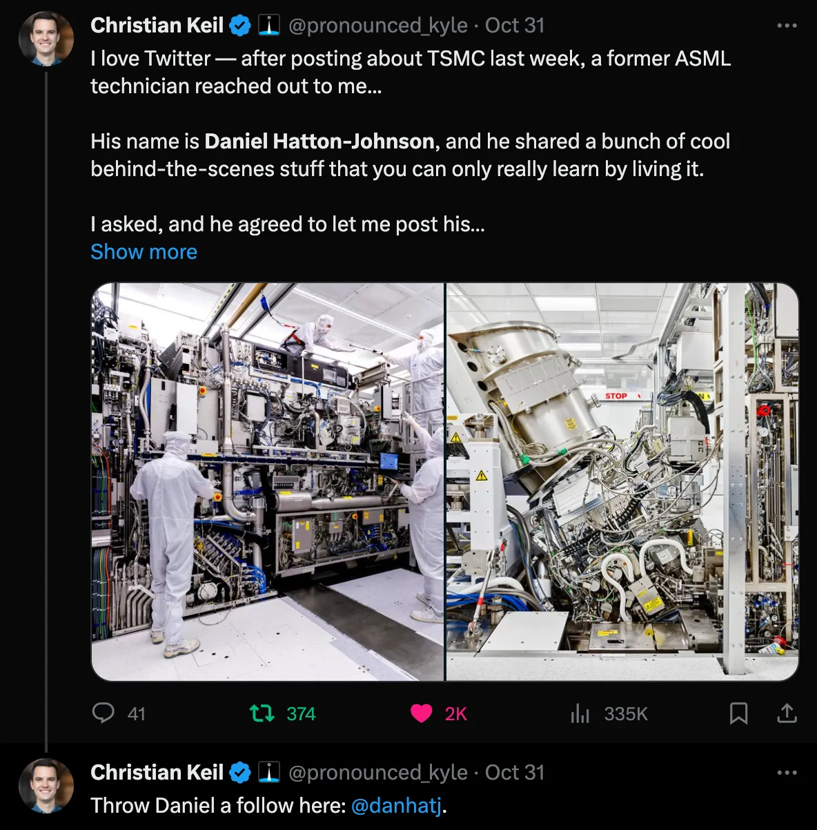
I love Twitter — after posting about TSMC last week, a former ASML technician reached out to me...
His name is Daniel Hatton-Johnson, and he shared a bunch of cool behind-the-scenes stuff that you can only really learn by living it.
I asked, and he agreed to let me post his message in full:
Hi Christian,
I saw your Tweet on TSMC and why what they do is so hard. There were so many good answers and recommendations.
Background
The reason I thought to write is that I have lived in Eindhoven in the Netherlands for the last four years. I came to start a deep tech company at an incubator here (another story).
On arrival in October 2019 I had no manufacturing or production experience at all, so I got a part time evening job at ASML whilst working on the company. Then the following year moved to a company called SMART Photonics, who make Photonic Integrated Circuits. A relatively tiny semiconductor company, that has raised around €100 million to date.
I’ll mostly summarize those experiences below. I currently work as a Quality Technician at VDL Enabling Technologies Group, where we make some of the smaller machines and modules that go inside the giant ASML machines. This includes the vessel, which is the thing that vaporizes the tin droplets to generate UV light. I literally work with those and two other machines every day, the atmospheric wafer handler and the vacuum wafer handler.
————————
Eindhoven eco system
One thing to note is that all of these companies came out of Philips, what was originally a lighting company before electronics and now mostly advanced medical equipment. Eindhoven is named the city of light. Not because of light bulbs, but because there was a huge match industry from the 1840’s to the 1920’s.
Both ASML and SMART spun out of Philips, whilst VDL- ETG was an acquisition by the VDL Group, a large Dutch industrial family business that also started as a single machine shop in Eindhoven in 1953, which included Philips among its first clients.
I gave this background because it gives some insight into the size and depth at least one chip making and industrial eco system here. For a long time it has attracted engineers, scientists and technicians from around the world. Then you have a very large supply chain to be able to build things and so it's easy to create companies that build things or service the companies that are building physical products. From basic things like chains, hoses, tractors and ceramics to advanced cooling, lasers and medical equipment.
Another fun fact is that Eindhoven has the highest concentration of patents per head of any city in the world. It also has the, by far, highest concentration of people with autism in the world as invention, autism, creativity and things like left handedness have been shown to be correlated. With the children of doctors and engineers the most likely to score highly for neurodivergent traits.
————————
Companies
ASML- I worked a basic technician job in a cleanroom of the servicing building so won’t elaborate too much there. We basically used to check and ship parts to fix machines that were installed globally.
VDL- I work on the two wafer handlers, the vessel and their spare parts. This role is fairly advanced manufacturing, but it's not too hard or intricate in comparison to making chips. The harder part is the design, iteration and prototyping when a new version of a machine gets built. Thereafter its a fairly steady, standardized process. It then goes to ASML where they have to get those things working to spec which is pretty hard as it requires small tolerances that rely on great software to get all of the moving parts talking to each other. That’s where it really becomes rocket science again.
SMART- Photonics - They are a foundry making tiny photonics chips. These chips are still relatively large compared to modern electronic integrated circuits. The reason being that light has a much longer wavelength than electrons do. The wavelength of light used in PICs is typically between 1500 nm and 1650 nm. This means that the features in a PIC must be at least as large as the wavelength of light in order to effectively guide and manipulate the light, always following a curve to take a smooth path and prevent reflection. In contrast, electrons have a much shorter wavelength, on the order of 0.1 nm so the feature size can get tiny. Meaning that the process is not just intricate, it’s unimaginably difficult to do and then to scale and have good yields. Any contamination like a tiny grain of dust on any layer can damage and destroy a photonics chip, and that same particle that would leave a photonics chip functional would likely destroy an electronic chip or two with such small feature sizes.
Much of our process was still similar and because of the larger feature size and being a lab to fab rather than a full chip fab, we did more experimentation and more manual handling than you’d ever see in a large scaled up electronic semiconductor plant. So you got to see a wafer start from the beginning, blank and then see layers added, or removed and transformed by the process. The base material for our foundry was mostly indium phosphide (InP), and sometimes gallium arsenide (GaAs) rather than silicon since as both materials are able to generate light. Though InP for example has comparatively high loss, compared to Silicon since it's such a great insulator meaning light propagates well though silicon waveguides. But they then need an external, usually larger light source.
With InP that can all be done on chip and [we were all in] on InP. Though the drawbacks are that the material is very brittle and the process is still not scaled like CMOS so we started with two and three inch wafers. The company has now moved to four inch wafers so with larger chips and smaller wafers, the yields don’t come anything close to electronic chips which tend to be about 12 inches across. So the costs are relatively high, but the applications such as quantum computing, sensing and detection cannot be done in silicon electronics, adding massive value to the areas where these chips are used.
As with silicon the production of a single finished wafer takes around 8-16 weeks and on the way there, there could be any number of challenges because you are using machines and materials that are undergoing nanoscale state changes. So for examples you may change the formula or your photoresist, or you could have two materials that interact well until there are changes in temperature with heating or cooling from the bake off process for example. Which could leave cracks in a layer of your chip because the materials could expand or contract at different rates or temperatures whilst being structurally connected.
Any metal or glass/silica waveguide on top of this could then have a short circuit in the electronic components and loss or scattering in the photonics components.
So you’d grow layers of InP in a huge reactor, do chemical etching, photolithography and a number of different process steps, adding and removing materials, building a working chip layer by layer.
The amount of processes involved are staggering. There are reactors for crystal growth which need to be connected to dangerous gases. This for us was generally done by experienced engineers and chemists/materials scientists who would go into those rooms with masks and oxygen tanks on. Then you have machines for photolithography that we mostly got from ASML.
These didn’t need to be top of the line due to larger feature sizes so we had older machines as they last a very long time. Then a newer one which is relatively cheap in the low tens of millions of euros.
Add to that ultra precise measuring and metrology equipment, SEM microscopes and other microscopes of varying strengths. The list of high tech machinery was endless. This all had to be maintained by experienced process engineers and technicians.
————————
The people
This is a summary of my experience as someone who was previously a layperson and went head first into this environment after a life of office work. I have a degree in sociology and did further study later in things like UX design and other things in digital and IT. Coming here was an expansive, mind bending experience. It’s like a totally different world compared to most cities.
I spent lots of time speaking to my colleagues and so many of these people were just incredible. They’d have to solve impossible problems constantly under pressure, in the middle of a batch that if ruined would take weeks to get back to the same place.
You could grab a colleague in the lunch room and ask anything about their area of expertise and the depth of knowledge and experience was generally unbelievably high. If you didn’t want to talk about work it could be a conversation about time dilation or any number of things related to the sciences as they are, or going over outstanding questions in science.
For some time I sat next to a guy who was a brilliant mathematician, trying to solve Goldbach's conjecture in his spare time. He believed only prime numbers were truly numbers as opposed to base 10, or base 12 number systems which as he said were largely culturally defined and arbitrary. That guy was incredibly interesting, as were many people there. The guy who swapped desks with him was trained in chemical engineering and was equally brilliant. These were two middle aged white guys who wore glasses and had a kind, calm demeanour, which makes you stop believing in both ageism and talented assholes as a pathway to success.
With companies like ASML and TSMC, they have many, many more of these individuals. In fact some of our best people had come from ASML and the large chip companies like NXP. But they generally wanted more freedom, creativity and a better work life balance as the big companies require a lot of overseas travel. Those people work under immense pressure and are pretty well compensated for it.
This is mostly personal experience and it’s a little short, but I wanted to at least give some insight from one part of the global semiconductor ecosystem here in Eindhoven. I’d be happy to either talk a little more, or try to put you in touch with a colleague or former colleague who knows more.
I also have a friend working at Schunk Xycarb in the next town over, which is a company specializing in Carbon manufacturing at scale. They grow the large crystals that become the wafers for semiconductor, which again is a highly specialized process in itself.
This whole thing is a huge, huge ecosystem, and the fabrication of chips, the epicenter of it, is probably the hardest part along with creating and operating the lithography machines at scale in a way that generates profits. I have missed entire areas like mask design, testing, reliability testing, logistics, transportation design, and delivery processes for multiple customers.
And that was it. Christian posts pretty cool content related to manufacturing and the mission of Astranis, launching communications satellites into orbit to connect the world.
How to Make Computer Chips from the Ground Up 2/3
Questions and answer below:
1) are the service providers for the components of manufacturing the same as those for more mundane components?
2) do both have/require military clearance/background checks?
3) do people from the fab industry transition there or do they remain separate?
4) what are the scale and speed at which they truly operate? Turnovers etc?
5) any anecdotes or tales you feel comfortable sharing are welcome, you have a nice way of writing.
-----------------
Another post after @tomethetemple asked me to elaborate specifically on semiconductor logistics. Additionally, here’s another article followed by a thread of photos describing a small part of the wider manufacturing eco system in and around the city: Eindhoven Eco System and infrastructure
Thanks again to @pronounced_kyle for sharing the letter I wrote in response to your post on TSMC, and for the 300 or so followers I gained the last few days. Hopefully this is just as insightful.
Q: Are the service providers for the components of manufacturing the same as those for more mundane components?
Different components of varying complexity are manufactured by different companies. A company doing finished assembly typically wouldn’t be manufacturing the smallest things like bolts, washers, hoses and screws. Those are generally bought in bulk from suppliers who specialise in those areas.
A large company like the VDL Group has many businesses that assemble products of varying complexity, it does not go down to the level of individual components unless they are large parts that go through CNC machines.
If a company is more high tech, they’ll assemble things that are at least at a minimum level of complexity, whereas a hose company may provide various types of rubber or metal hoses that adhere to strict tolerances and cleanliness as required per part.
The same would go for bolts, screws, washers and other singular pieces. One supplier would likely try to look for economies of scale in certain parts. But again, they may supply to a vehicle manufacturer with no clean room grade or approval needed at all.
Those same bolts or hoses would need certification and supplier approval so that you know they have a process in place to ship those simple parts at scale to cleanrooms. In some cases for the highest cleanliness grade, meaning they would have to arrive with zero particles or contamination of any kind.
For this, there’s a company called HQ pack that has buildings around the city supplying many of the local companies.
Either way, things look similar on the factory floor of a cleanroom and of normal factories. Stackable plastic ‘RAKO’ boxes full of general parts are stored in the factory to match orders.
Often the standard small parts like screws, bolts and washers will always be in stock, whereas other parts tend to come in for the particular machine or process, even hoses as different lengths are required depending on the type and model of machine you are building.
Q: Do both have/require military clearance/background checks? And any anecdotes...
ASML (Part time whilst at inPhocal) - For this role I did require a background check from the local municipality as we would be handling parts from this service building that may go by air freight once they left the warehouse. Not to mention we were handling sensitive, crucial and sometimes incredibly expensive parts from the lithography machines.
For a short period of maybe two weeks before starting at SMART Photonics I worked on the other side of the building ASML shared with DHL, split so that DHL could handle the logistics for trucking and air freight etc, while ASML warehouse employees would organise their side and sort products to go into and out of the adjacent cleanroom, where they would be processed at different grades of cleanliness.
Most of the ASML warehouse employees could operate the forklifts and other electronic vehicles as well as having the training to work in the cleanroom, so everyone would work between both as demand required. Myself included.
In addition to a new background check for this temporary role, I had a certificate that allows you to deal with air freight and we worked in a separate area of this huge warehouse in a giant cage that had a wall length electronic gate which was only opened and closed when materials or people were moved in and out of it.
Next I went to SMART Photonics, where I eventually moved into quality after working in a general logistics role. ASML and DHL are both huge companies, but at SMART I was employee number 77.
Life at a scale up proved to be very different and gave huge opportunities for learning across all departments as the company grew.
Back then at SMART we had a couple of little cars, I would transport small amounts of materials and tools between two production sites, as well as any other work that needed to be done in our department.
As I’m a bit of a generalist this did include ordering equipment and materials for our cleanroom along with a colleague who later joined from ASML. We were very familiar with the clean pack and contamination control best practices after our time there.
The SMART Photonics office and cleanroom are still based at the former Philips research Lab, now called the High Tech Campus, in building 29, though I think they recently moved due to continued expansion. It’s the same building where the Blue Ray disc was invented, for those old enough to know Physical CDs for movies.
This job was pretty handy as inPhocal is based in a building just across the way, HTC 27, in the offices of the incubator, High Tech XL. That way it was still easy to work full time and attend meetings or events around working hours.
After some time I moved from logistics to a combination of that and quality technician. I would move materials and inspect them as they were going through the line, but it was mostly end of line once they were ready to ship.
Unless there was an issue during production, in which case I would get an emergency batch from the line, or from R&D. This could well be a lot of work at the last moment, but that’s how things go in manufacturing, which compared to any previous job I’d had was very high stakes. Especially when scaling a new technology.
After 2.5 years at SMART Photonics I got a new role at VDL Enabling Technologies Group, the place where the smaller ASML machines and modules are built. That includes the part that generates the UV light by vaporizing tin, the vessel, and the smaller wafer handler.
Again, just before starting there, I took an in-between role at another VDL company, VDL Bus and Coach which is just south of the city. This was a big departure from high tech, and was only for one month but it was incredibly insightful in that short time as I’ll elaborate on below:
Q: What are the scale and speed at which they truly operate? Turnovers etc?
The scale and speed that a company operates really does depend. With ASML it was just parts, tools and carriers for servicing machines. A lot moved through that building on a daily basis, but it's hard to say exactly how much of what because of the fact it was just parts and a section of a machine at most.
The same goes for DHL which was colocated for the actual transit in and out of the trucks for road and air freight, in a huge shared/split warehouse.
Then at SMART, as its a chip foundry you’d have wafers moving through multiple stages and taking (ideally) 8-12 weeks to finish as you added different materials and put them through different processes. That’s the most complex thing I’ve personally seen being made.
Wafers are constantly going through different processes in the production line and at the end of the line involving measuring tools and microscopes. As nano structures you can’t just look at the physical parts in the same way you would with a large human scale machine.
It was also a very new technology so the company was transitioning ‘from lab to fab’, that is working at the intersection of research and scaling quantum materials into everyday use.
At VDL they do contract manufacturing, so most of the invention and design would be done by, or with the customer. Then it was building and process. While it is high tech the business was more about units through the door. Which is itself a very hard process.
I’d seen carriers for parts before, but had no idea how complex and truly massive, the carriers and tools could be for these large machines. It was mind boggling.
You’d have tool engineers designing tools and lockings that would keep the machines steady in transit and allow you to lift them with cranes and other interesting ways of moving sometimes huge things around and then outside.
The smaller, less complex machines can go out at far higher rates than the bigger ones. Those are both harder to build, harder to mount and harder to move. they also require longer more detailed physical checks and testing by more experienced people.
For example, You might expect a line to produce 10 of the simpler machines per week, Perhaps five per week of an intermediate machine and 1-2 of the largest most complex machines. Which is staggering if you think about it. This is assuming a warm start and a line full of partially assembled machines.
So some things are built in the scale of weeks, and some are built in days. Interestingly, the biggest and smallest things are what take the most time, since those are the places where there is most complexity.
In my experience, the Vessel (UV light source for lithography) and more so a photonics chip were the hardest things I’ve seen being put through production.
Watching the buses being made was really cool because of the scale. I worked in the diesel hall but would go over to the new hall to watch the electric bus line and ask the technicians and engineers questions.
Electric assembly had far fewer moving parts. Those frames looked so much more elegant and there was just less of everything compared to diesel.
It was also very clean compared to the diesel hall, but still nothing like a cleanroom. However the difference there was stark when going from one side to the other.
The diesel line had slowed from its heyday so I came to learn. The guys were putting out impressive numbers before things stopped due to covid, and then came the immediate transition to electric vehicles as customers pivoted towards sustainability.
In the diesel hall, a frame would come in from a company down the road and then you’d literally see every last part added. Axels, suspension, wheels and engines would be fitted. The AC system, and then windows. Then in the next part of the line carpets, flooring, the toilet system and onwards.
That was fascinating because everybody kind of understands vehicles as we see them everyday, but seeing one built from scratch and seeing the components as they come in and then go into a bus was pretty cool.
I couldn’t choose which line was more fun to watch as they were both fascinating for different reasons. There is nothing like being part of a process where you create real things, which is the same for most of the companies here.
Buses and coaches lacked the prestige of semiconductor and mechatronics. But seeing vehicles rolling off of the line and then driving out of the factory to go and carry people around cities and countries was intensely satisfying.
Q: Do people from the fab industry transition there or do they remain separate?
Yes people do change industry because so much of it is just process and understanding how to implement those processes. This would typically be easiest in the warehouse logistics because that doesn’t vary too much between companies.
But I did have colleagues move from Mars (Chocolate/sweets) and Friesland Campina (Dairy) move into the high tech sector. Of course it takes time to get familiar with a new industry.
That said, the more experience you have in a certain industry the better. Especially semiconductor, where the most senior and/or experienced technicians have the same or higher salaries than some engineers depending on seniority.
I moved from quality in semiconductor to quality in mechatronics. Semiconductor fabrication was far more interesting and we got to use better tools, but the process, reporting and feedback was pretty similar.
Q: Do people move around between companies?
Yes. My first job was at ASML. At SMART Photonics two former colleagues, technicians from ASML then joined. Of course there are other people with more past connections from other companies but this is my experience.
At VDL ETG, I was joined by two former colleagues from SMART Photonics, and three from ASML, so yes it’s incredibly common to move around companies that are in the same, similar or complimentary industries.
For example semiconductor mechatronics at VDL ETG and semiconductor chip fabrication at SMART Photonics are very complimentary for many processes.
Specialists, like materials scientists and chemical engineers would likely stay in semiconductor though. Specialist research scientists who work with nanostructures, crystal growth and layer deposition would probably stay in semicon too as would the experienced process technicians.
It’s more complicated, specialised and lucrative than some other general engineering processes.
Most lucrative and opportunity laden of all though is ASML. After the slow decline of Philips, which built this city and supply networks with partners, ASML grew to become the new local, regional, continental and global behemoth.
The question is who is next, or will ASML continue to innovate beyond lithography into new areas over the next 20-30 years
Or what companies will end up spinning out of ASML in the next half century as ASML, VDL ETG (Acquirer of Philips ETG), SMART Photonics, NXP semiconductor and others that came out of Philips. We seem to live in a predictably unpredictable world.
How to Make Computer Chips from the Ground Up 3/3
Part two of the Tweet reply:
@tomethetemple asked me to elaborate specifically on the logistics side of the semiconductor industry. That’s here: Part 2/3 Tweet
Thanks again to @pronounced_Kyle for sharing the letter I wrote in response to your post on TSMC and to the 300 new followers. Hope this interests you.
——————————————
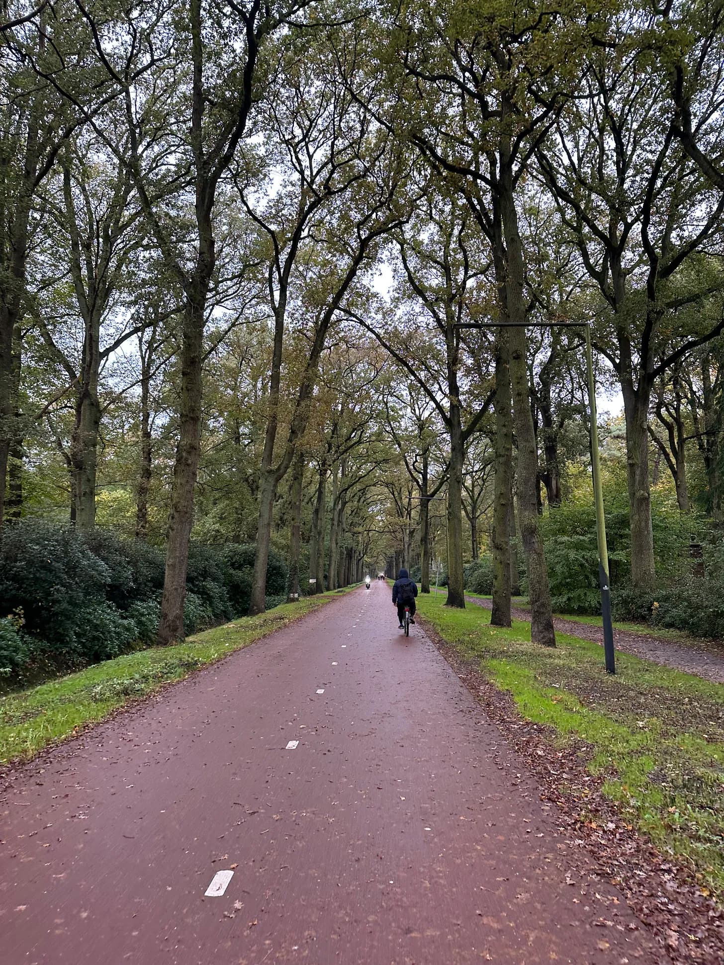
Last Wednesday, instead of taking my usual morning ride of (+/- 35km) in the surrounding countryside, I rode from my house around the city in order to show how Dutch urban planning contributes to being able to move things and people. Proving that it’s possible to have a liveable city with a high density of industry.
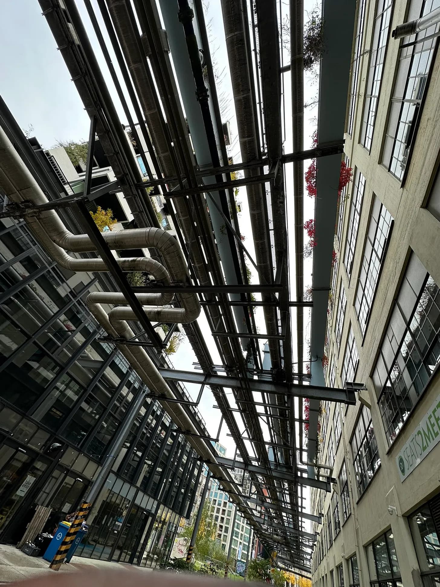
I started in my neighbourhood, Strijp-S, where the first Philips glass factory (For light bulbs) was built in 1916. The site then expanded to radio, television, research facilities and box factories to ship finished goods. The credo at Philips was ‘from sand to customer’ or ‘Van zand tot klant’ in Dutch.
Many of the buildings are now offices, apartments, restaurants, small production workspaces, even including an indoor skate park. Much of the industrial character, like the gas pipes remain to preserve the character of the site. *See Strijp-S images in thread Next I went north through the Park to my most recent work place VDL ETG, showing the surrounding business, many of whom work together and support one another in the creation and movement of raw materials and finished goods to local, regional and global customers.
*See Philips De Jongh Park images in thread
This scenic ride is around 15-20 minutes and 2.5 miles (4km) from Strijp-S. I entered at the entrance closest to the highway so I could do a loop through and show a handful of the companies as I went.
First is Jan Tromp Logistics, a local transportation co that serves Eindhoven industry and surrounding regions. This building is opposite the highway going North to Amsterdam and the other larger Dutch cities. The highway also goes to Belgium and Germany, within 30 minutes, and one hour respectively.
Next was HQ pack, one of the most important companies for high-tech, as they provide packaging for clean room environments. Any company producing sensitive equipment, in semiconductor for example needs their packaging to get products in and out of their clean rooms. There are levels of cleanliness according to specific parts and their place within a machine.
Entire machines have gradings as they move through the production process. Humans also have to wear full body suits to stop contaminants like grease, hair, skin and body fluids, even at small concentrations.
There are companies who supply thousands of clean room suits, and companies to do cleanroom laundry for thousands of suits per week.
Next I went around to VDL ETG, where high tech modules are assembled in their totality. VDL ETG also does machining/cnc of very large metal components.
Across the road is Volkswagen, MAN trucks for business customers. Scherpenheizen (packaging of fresh produce). The Netherlands, despite being the 131st country in terms of land area, is the worlds second largest agricultural exporter behind the United States at #1.
Technische Unie, A technical wholesaler that sells many parts needed in industry of all types from production to construction, and on to Galvano metaal, the next company along which will deliver any orders of metal over 10 tons, the same day.
Further along I passed Thermo Fisher Scientific’s centre for electron microscopy, essential because while you need machines, you’ll also need finer measuring equipment like microscopes.
At SMART Photonics I was lucky enough, for the first time in my life to have a really good (KEYENCE) microscope as my dedicated work tool, which would typically cost somewhere in the region of €200k. Essential for looking at nanostructures on chips.
Across the road from Thermo Fisher you have another logistics company, Van Rooijen logistics, which ships everything from food to pharma, cosmetics and displays.
This huge warehouse even has its own rail terminal connecting to the mainline going north west to the large Dutch cities, Utrecht, Amsterdam, The Hague and Rotterdam, and south and south east to Aachen, Dusseldorf and Cologne in North Rhine Westphalia, Germany. The country’s largest and most populous economic region.
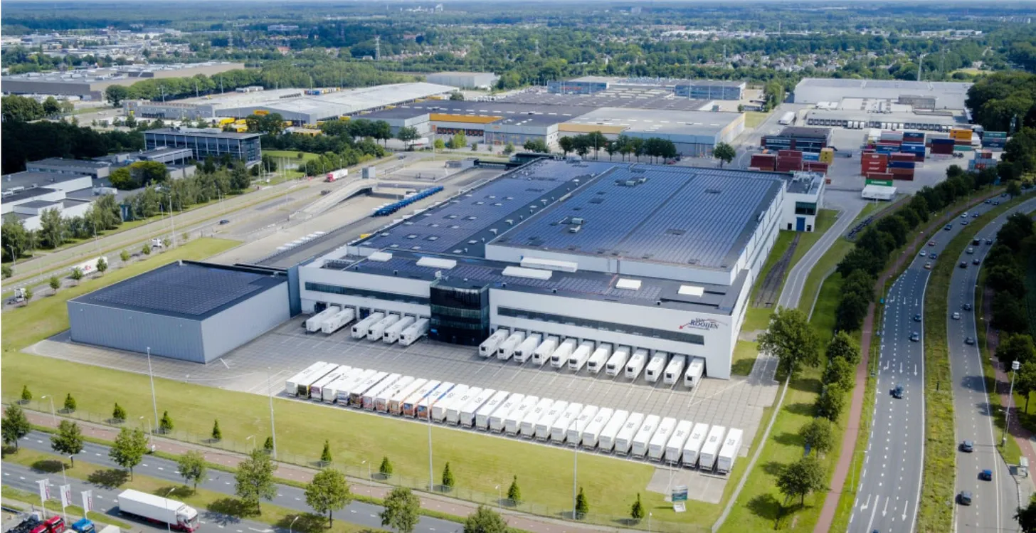
At the end of the road are two large distribution centres, DHL and UPS, the latter was newly built in 2017 and is able to handle 29,000 parcels per hour. This building was built by another regional company, Geelen.
In the attached thread, a plane flies over UPS to the airport which is a 20 minute bike ride away from this site. This one site shows the levels of integration of road, rail, air and cycle ways to move people and goods around efficiently.
Both locally and with direct connections by road and rail to two of Europe’s largest economic regions in NRW in Germany and the Randstand in Holland next to neighbouring Belgium, where you have three of Europe’s five busiest ports, Rotterdam, Antwerp and Amsterdam.
Next I rode down to De Hurk, a four mile (6km) 22 minute cycle to the west of the city. Both sites are next to the ring roads of the inner part of the city proper with easy access to the highway, to give some perspective.
Down in De Hurk, I passed another VDL group building, VDL GL Precision which make smaller precision parts for everything from optics to automotive and again semiconductor.
Riding along I passed an equipment rental company, Boels then got to some of the larger HQ pack buildings as this is where their headquarters is located. Without this company, things just wouldn’t stay clean in transit, so they are a crucial part of the supply chain in high tech manufacturing.
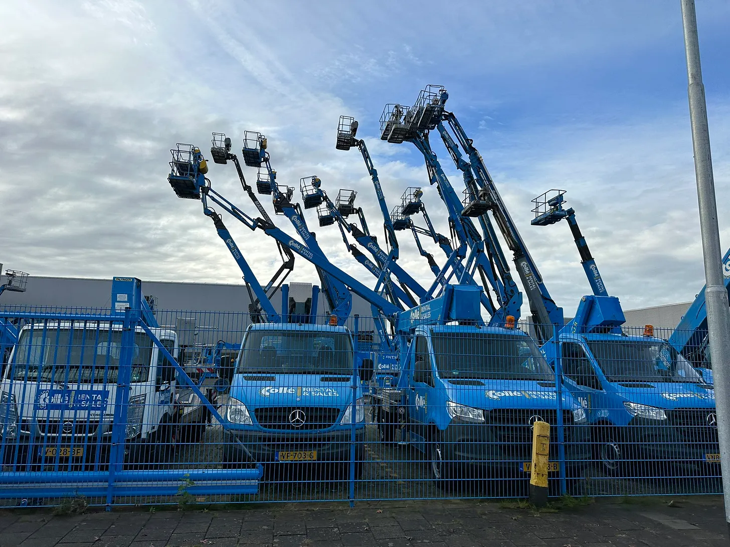
Just around the bend you have Colle rentals, who rent equipment. More on them later. After Colle you have Air Liquide who supply various type of gases for production process. This is also a very crucial part of the supply chain, particularly in the semiconductor business for things like reactors.
Further on and going past too many businesses to mention, I pass another VDL company, VDL ETG precision on the corner, diagonally opposite to a very small ASML building. ASML has buildings all over Eindhoven, mostly in the next town over, Veldhoven and those are as huge as they are numerous.
Over this road I get to one of the final pieces of he transportation system, the Canal. Numbers were hard to find for this canal, but I did see that the Netherlands has the largest inland shipping fleet in Europe, carrying 35% of national tonnage, of which 80% is bulk cargo transport. In total, 40% of the EU’s inland container shipping passes through the Netherlands.
Next I cycle from here back to the city centre (15 minutes) and I go through the centre to head south to the DAF trucks factory. This entire journey has been on separated bike lines, or some that are split with roads. they tend to split and merge in very fluid ways.
*See City images in thread
DAF is one of the largest truck manufacturers in Europe, making 70,000 trucks per year. They also make and ship engines (PACCAR) to other companies building large vehicles like trucks, busses and coaches. Seattle (U.S) based PACCAR has owned DAF trucks since 1996.
As I get closer I can see one of the local waste companies Renewi has a truck and the hydraulics on the waste truck are made by one of the VDL companies.
The truck then drives into the DAF factory, I presume for servicing. I see other trucks driving in and out, and every so often you’ll see new trucks leaving in fleets for delivery to customers.
I headed back to the centre to finish my ride at Eindhoven Centraal train station. At the back of the station is the bus station. Every bus here aside of one (Volvo) is manufactured by VDL bus and coach in a place called Valkenswaard, just (14km/9 miles) south of the city.

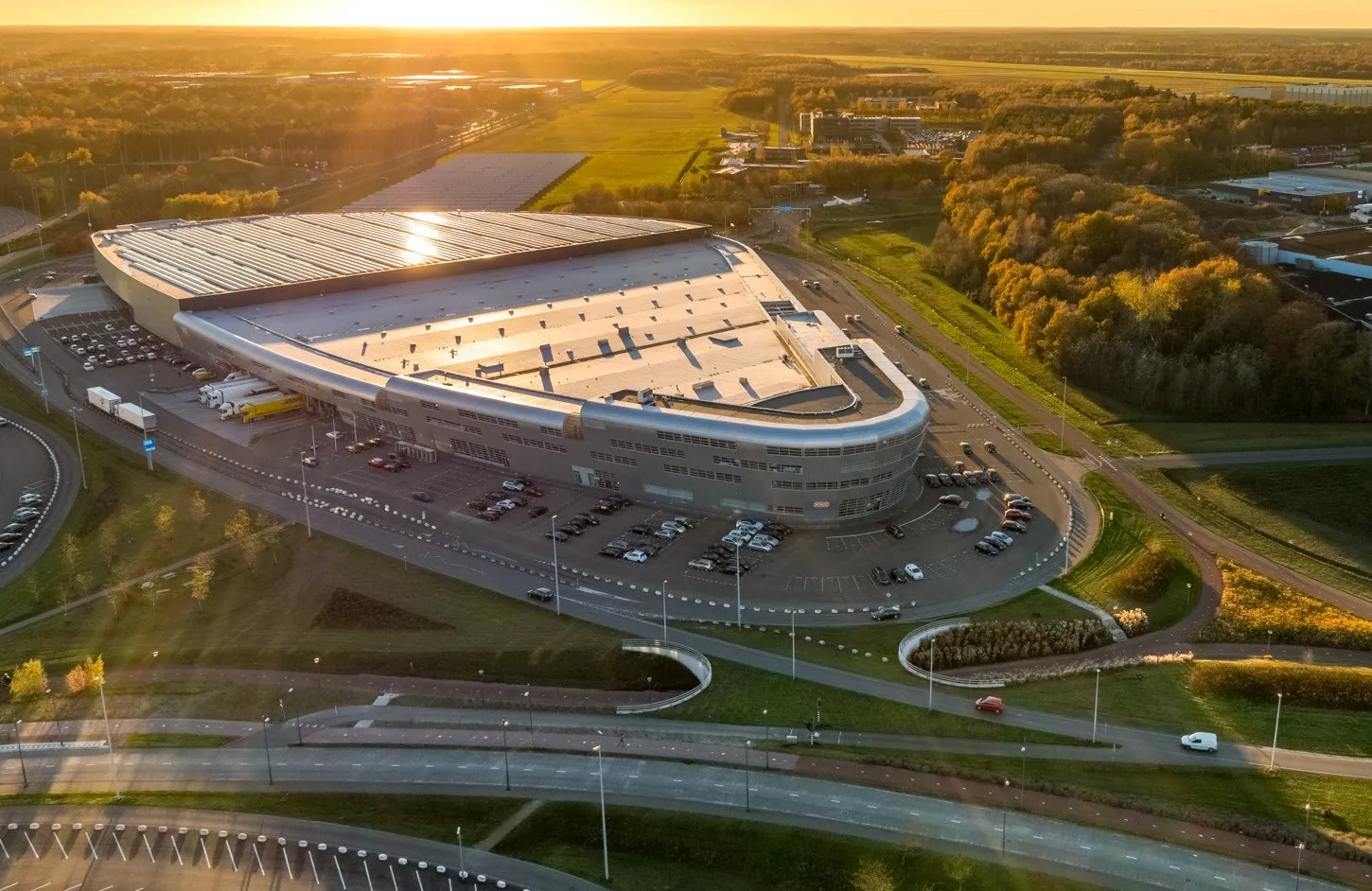
I finish at Media Markt, where Tim Cook recently had an interview as he visited in September to meet with an Apple supplier NXP semiconductors, which has an HQ on the High Tech Campus.
Back to the crane rentals, because as I rode around I saw them being used for maintenance around the city, including for the stadium of PSV Eindhoven. They were also being used in the city centre, in Strijp-S and by the library and design school.
Building a highly functional society is hard, but its the maintenance and upkeep with such a fast pace and consistency that’s all the more impressive.
When it snows potholes may appear or road surfaces can break up. As soon as the snow clears they are fixed within a day or two.
On a snow day the main cycle lanes in and around the city are cleared multiple times per day so people can still get around by bicycle.
In January I had a 14km daily commute from Strijp-S down to VDL Bus and Coach in Valkenswaard. I used to do a similar journey by car before moving into the city, but it’s just as easy on a bike all year round.
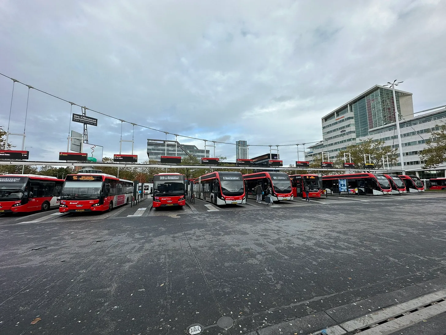
VDL buses at Eindhoven Bus Station
Get In Touch
Have questions or comments about this content? Feel free to reach out.